- 您现在的位置:买卖IC网 > Sheet目录369 > W971GG6JB25I (Winbond Electronics)IC DDR2 SDRAM 1GBIT 84WBGA
�� �
�
�W971GG6JB�
�10.12� AC� Input� Test� Conditions�
�CONDITION�
�Input� reference� voltage�
�Input� signal� maximum� peak� to� peak� swing�
�Input� signal� minimum� slew� rate�
�SYMBOL�
�V� REF�
�V� SWING(MAX)�
�SLEW�
�VALUE�
�0.5� x� V� DDQ�
�1.0�
�1.0�
�UNIT�
�V�
�V�
�V/nS�
�NOTES�
�1�
�1�
�2,� 3�
�Notes:�
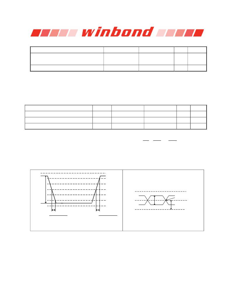
�1.� Input� waveform� timing� is� referenced� to� the� input� signal� crossing� through� the� VIH/IL(ac)� level� applied� to� the� device� under� test.�
�2.� The� input� signal� minimum� slew� rate� is� to� be� maintained� over� the� range� from� VREF� to� VIH(ac)� min� for� rising� edges� and� the�
�range� from� VREF� to� VIL(ac)� max� for� falling� edges� as� shown� in� the� below� figure.�
�3.� AC� timings� are� referenced� with� input� waveforms� switching� from� VIL(ac)� to� VIH(ac)� on� the� positive� transitions� and� VIH(ac)� to�
�VIL(ac)� on� the� negative� transitions.�
�10.13� Differential� Input/Output� AC� Logic� Levels�
�PARAMETER�
�AC� differential� input� voltage�
�AC� differential� cross� point� input� voltage�
�AC� differential� cross� point� output� voltage�
�SYM.�
�V� ID� (ac)�
�V� IX� (ac)�
�V� OX� (ac)�
�MIN.�
�0.5�
�0.5� x� VDDQ� -� 0.175�
�0.5� x� VDDQ� -� 0.125�
�MAX.�
�VDDQ� +� 0.6�
�0.5� x� VDDQ� +� 0.175�
�0.5� x� VDDQ� +� 0.125�
�UNIT�
�V�
�V�
�V�
�NOTES�
�1�
�2�
�3�
�Notes:�
�1.� VID� (ac)� specifies� the� input� differential� voltage� |VTR� -VCP� |� required� for� switching,� where� VTR� is� the� true� input� signal� (such�
�as� CLK,� LDQS� or� UDQS)� and� VCP� is� the� complementary� input� signal� (such� as� CLK� ,� LDQS� or� UDQS� ).� The� minimum�
�value� is� equal� to� VIH� (ac)� -� VIL� (ac).�
�2.� The� typical� value� of� VIX� (ac)� is� expected� to� be� about� 0.5� x� VDDQ� of� the� transmitting� device� and� VIX� (ac)� is� expected� to� track�
�variations� in� VDDQ.� VIX� (ac)� indicates� the� voltage� at� which� differential� input� signals� must� cross.�
�3.� The� typical� value� of� VOX� (ac)� is� expected� to� be� about� 0.5� x� VDDQ� of� the� transmitting� device� and� VOX� (ac)� is� expected� to�
�track� variations� in� VDDQ.� VOX� (ac)� indicates� the� voltage� at� which� differential� output� signals� must� cross.�
�V� DDQ�
�V� IH(ac)� min�
�V� IH(dc)� min�
�V� SWING(MAX)�
�V� REF�
�V� IL(dc)� max�
�V� TR�
�V� DDQ�
�V� IL(ac)� max�
�V� SS�
�V� CP�
�V� ID�
�Crossing� point�
�V� IX� or� V� OX�
�Δ� TF�
�Δ� TR�
�V� SSQ�
�Falling� Slew� =�
�V� REF� -� V� IL(ac)� max�
�Δ� TF�
�Rising� Slew� =�
�V� IH(ac)� min� -� V� REF�
�Δ� TR�
�Figure� 28� –� AC� input� test� signal� and� Differential� signal� levels� waveform�
�Publication� Release� Date:� Sep.� 24,� 2013�
�-� 66� -�
�Revision� A09�
�发布紧急采购,3分钟左右您将得到回复。
相关PDF资料
W971GG8JB-25
IC DDR2 SDRAM 1GBIT 60WBGA
W9725G6IB-25
IC DDR2-800 SDRAM 256MB 84-WBGA
W9725G6JB25I
IC DDR2 SDRAM 256MBIT 84WBGA
W9725G6KB-25I
IC DDR2 SDRAM 256MBIT 84WBGA
W972GG6JB-3I
IC DDR2 SDRAM 2GBITS 84WBGA
W9751G6IB-25
IC DDR2-800 SDRAM 512MB 84-WBGA
W9751G6KB-25
IC DDR2 SDRAM 512MBIT 84WBGA
W9812G6JH-6I
IC SDRAM 128MBIT 54TSOPII
相关代理商/技术参数
W971GG6JB-25I
制造商:Winbond Electronics 功能描述:-40~85 1GB DDR2 FOR INDUSTRY
W971GG6JB25ITR
制造商:Winbond Electronics Corp 功能描述:1G, DDR2-800, X16, IND TEMP
W971GG6JB25TR
制造商:Winbond Electronics Corp 功能描述:NR, DDR2-800, X16
W971GG6JB-3
制造商:Winbond Electronics Corp 功能描述:1GBIT DDRII
W971GG6KB-18
制造商:Winbond Electronics Corp 功能描述:1G, DDR2-1066, X16 制造商:Winbond Electronics Corp 功能描述:IC MEMORY
W971GG8JB
制造商:WINBOND 制造商全称:Winbond 功能描述:16M × 8 BANKS × 8 BIT DDR2 SDRAM
W971GG8JB-25
功能描述:IC DDR2 SDRAM 1GBIT 60WBGA RoHS:是 类别:集成电路 (IC) >> 存储器 系列:- 标准包装:72 系列:- 格式 - 存储器:RAM 存储器类型:SRAM - 同步 存储容量:4.5M(256K x 18) 速度:133MHz 接口:并联 电源电压:3.135 V ~ 3.465 V 工作温度:0°C ~ 70°C 封装/外壳:100-LQFP 供应商设备封装:100-TQFP(14x20) 包装:托盘
W9725G6IB-25
功能描述:IC DDR2-800 SDRAM 256MB 84-WBGA RoHS:是 类别:集成电路 (IC) >> 存储器 系列:- 标准包装:1,000 系列:- 格式 - 存储器:EEPROMs - 串行 存储器类型:EEPROM 存储容量:4K (512 x 8) 速度:400kHz 接口:I²C,2 线串口 电源电压:2.7 V ~ 5.5 V 工作温度:-40°C ~ 85°C 封装/外壳:8-SOIC(0.173",4.40mm 宽) 供应商设备封装:8-MFP 包装:带卷 (TR)